This example shows how ClearSCADA might be configured to act as a Modbus PLC, in order to report its data to a Modbus Master, using the Modbus protocol.
Example:
A ClearSCADA system is to emulate a Modbus PLC. The Modbus addressing starts at 1 (ClearSCADA addressing starts at zero.) The ClearSCADA database is to be configured so that ClearSCADA can transmit data for the following items to its Modbus Master:
- Input Registers 300001 and 300006
- Coils 5 and 9.
Within ClearSCADA, a Modbus Slave Channel is suitably configured to transmit data to the Modbus Master.
A Modbus Slave Source is configured to emulate a Modbus PLC and to use the above channel. In this particular example, the Source is assigned the Modbus address 19.

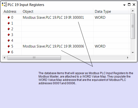
In a Modbus PLC, Input Register data is allocated in Words. Within ClearSCADA, a WORD Value Map is configured to emulate the Input Register memory area. As ClearSCADA is to transmit data for Input Registers 300001 and 300006, addresses 0 and 5 of the WORD Value Map are populated with the database items that represent those Input Registers. (WORD Value Map address 0 is the equivalent of Modbus address 1, and WORD Value Map address 5 is the equivalent of Modbus address 6.)

In order for the WORD Value Map to represent Input Register data, the Value Map (named ‘PLC 19 Input Registers’) is specified as the Input Register Map property on the Modbus Slave Source Form.

This sets ClearSCADA to transmit the WORD Value Map data as Input Register data. It also means that the entries that populate the WORD Value Map emulate Modbus PLC addresses 300001 and 300006.
In a Modbus PLC, Coil data is allocated in Bits.
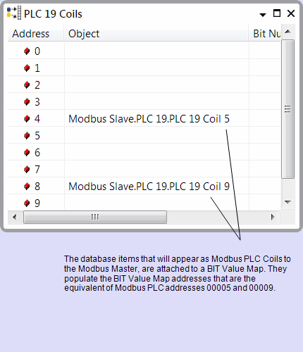
Within ClearSCADA, a BIT Value Map is configured to emulate the Coil memory area. As ClearSCADA is to transmit data for Coils 5 and 9, addresses 4 and 8 of the BIT Value Map are populated with the database items that represent those Coils.(Where Modbus addressing starts at 1, BIT Value Map address 4 represents Modbus address 5, and BIT Value Map address 8 represents Modbus address 9.)

In order for the BIT Value Map to represent Coil data, the Value Map (named ‘PLC 19 Coils’) is specified at the Coil Map property on the Modbus Slave Source Form.

This sets ClearSCADA to transmit the BIT Value Map data as Coil data, and means that the entries that populate the BIT Value Map emulate Modbus PLC addresses 5 and 9.
Further Information
Configuring a Modbus Slave Channel.
Configuring a Modbus Slave Source.
Using Value Maps to Represent Modbus Data Address Ranges.
Configuring BIT Value Maps and WORD Value Maps: see Configuring Value Maps in the ClearSCADA Guide to Core Configuration.